
CEM
3D Electromagnetics
Eigenmodes of a Superconducting Qubit Grid
A Multi-Qubit QPU on Anisotropic Sapphire, Solved with the Palace Finite-Element Solver
Explore GPU-accelerated computational electromagnetics (CEM) powered by NumericalAI and the open-source Palace 3D finite-element solver. Designing a quantum processor means knowing — before fabrication — exactly where each qubit and coupler will resonate. An eigenmode analysis finds those natural frequencies and field patterns directly from the layout, no drive signal required, by solving the source-free curl-curl eigenproblem.
This example models a grid of superconducting qubits patterned on a sapphire chip. Each qubit's Josephson junction is represented as a lumped inductor–capacitor (LC) port, and Palace computes the collective, hybridized modes of the whole array near the transmon operating band. The result is a full-wave picture of how energy distributes across the chip — the foundation for predicting qubit frequencies, couplings, and stray resonances.
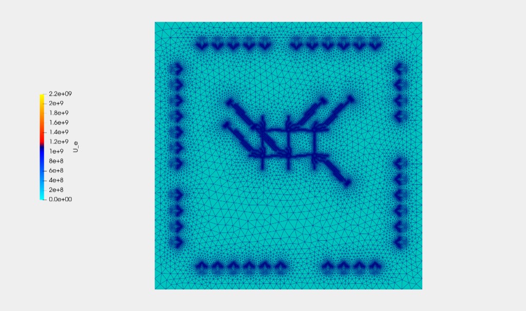
Electric energy density (U_e) of a computed eigenmode across the qubit lattice and its coupling network, on the meshed sapphire chip.
What the Model Represents
Qubits as Lumped LC Ports
Twelve lumped ports stand in for the Josephson junctions of the qubits. Each is a linearized junction: an inductance L = 14.86 nH shunted by a capacitance C = 5.5 fF, oriented along +Y across the junction gap. In the small-signal (linear) limit this is exactly how a transmon presents itself to the surrounding electromagnetic environment.
A Coupled Array, Not Isolated Qubits
Because all twelve ports share the same chip, the eigensolver returns the hybridized modes of the full grid — collective resonances in which energy is shared between neighbouring qubits and their coupling structures. This is what turns a set of nominal qubit frequencies into the real, coupled spectrum that governs gate performance and crosstalk.
Simulation Configuration
Geometry & Mesh
Structure:
Multi-qubit QPU grid
Qubit ports:
12 lumped LC
Length unit:
µm (L₀ = 1e-6)
Mesh:
Tetrahedral
Element order:
1
Substrate (Sapphire)
Permittivity (in-plane):
9.3
Permittivity (c-axis):
11.5
Anisotropy:
Uniaxial, rotated axes
Loss tangent:
3e-5 / 8.6e-5
Vacuum region:
εᵣ = µᵣ = 1.0
Solver
Problem type:
Eigenmode
Eigenpairs:
2
Target:
4.0 GHz
Inner solver:
GMRES + AMS
Tolerance:
1e-6
Boundary Conditions
Lumped ports (×12):
L = 14.86 nH, C = 5.5 fF, direction +Y
Metal:
PEC (superconducting electrodes & ground)
Enclosure:
First-order absorbing (radiation) boundary
Computational Setup
12
Qubit LC Ports
4 GHz
Target Band
~10 min
GPU Solve Time
AMS
Auxiliary-Space PC
Junction & Material Parameters
| Parameter | Value | Role |
|---|---|---|
| Junction inductance L | 14.86 nH | Sets the Josephson (kinetic) energy of each qubit |
| Shunt capacitance C | 5.5 fF | Sets the charging energy / anharmonicity |
| Substrate εᵣ (in-plane) | 9.3 | Sapphire dielectric — loads the resonances |
| Substrate εᵣ (c-axis) | 11.5 | Uniaxial anisotropy of the crystal |
| Loss tangent tan δ | 3–8.6 ×10⁻⁵ | Ultra-low dielectric loss → high coherence |
| Number of qubit ports | 12 | Size of the coupled array |
The lumped L and C linearize each Josephson junction; the solver targets the lowest modes near 4 GHz, the operating band of transmon qubits. Sapphire's tiny loss tangent is why it is a workhorse substrate for high-coherence quantum hardware.
Reading the Physics
Anisotropic Substrate Matters
Sapphire is not an isotropic dielectric — its permittivity differs along the crystal c-axis (11.5) versus in-plane (9.3), and the model even rotates the material axes to match the wafer cut. Capturing this anisotropy is essential: it shifts qubit and resonator frequencies by amounts far larger than the fabrication tolerances engineers are trying to hit, so an isotropic approximation would mis-predict the spectrum.
Energy Participation & Coherence
The energy postprocessing over the substrate reports how much of each mode's electric energy sits inside the lossy dielectric — the participation ratio. Combined with the loss tangent, this is the quantity that sets the dielectric-limited quality factor and, ultimately, qubit coherence times. The energy-density map above shows exactly where the fields concentrate, and therefore where loss and stray coupling will originate.
Where This Applies
Quantum Processor Design
Predict qubit and coupler frequencies of a full chip layout before fabrication, and catch frequency collisions early in the design cycle.
Crosstalk & Coupling
Quantify how neighbouring qubits hybridize and share energy, informing coupler design and gate-error budgets across the array.
Coherence Budgeting
Use dielectric participation ratios and loss tangents to estimate dielectric-limited Q and guide substrate and geometry choices.
Readout & Resonators
Extend the same eigenmode workflow to readout resonators, Purcell filters, and bus cavities that share the chip with the qubits.
Why NumericalAI for Quantum Hardware
Powered by Palace — AWS's open-source, GPU-accelerated 3D finite-element solver for full-wave electromagnetics
Lumped-port junctions — model transmon qubits and couplers as LC elements directly inside the full-chip solve
Anisotropic materials — capture sapphire's uniaxial permittivity and rotated crystal axes for accurate frequencies
Energy participation postprocessing — the loss and coherence metrics that matter for quantum hardware, on cloud GPUs
Business Value & ROI
NumericalAI brings production-grade electromagnetic simulation to an intuitive cloud interface — no solver installation, no cluster administration, no meshing bottleneck.
Tape out with confidence: verify qubit frequencies, couplings, and dielectric loss across a full multi-qubit chip in a single GPU run, catching costly frequency collisions before a wafer is ever fabricated.
Ready to Model Your QPU?
Run full-wave eigenmode simulations of superconducting qubit chips with Palace on NumericalAI. Upload your Palace config.json and mesh, and get mode frequencies and field maps on cloud GPUs.
AI-Assisted GPU-Powered Simulations
© 2026 NumericalAI, all rights reserved. |Privacy Policy |Terms of Service |Executive brief |CEM vs HFSS |FAQ